
Fast PCB Prototyping Service
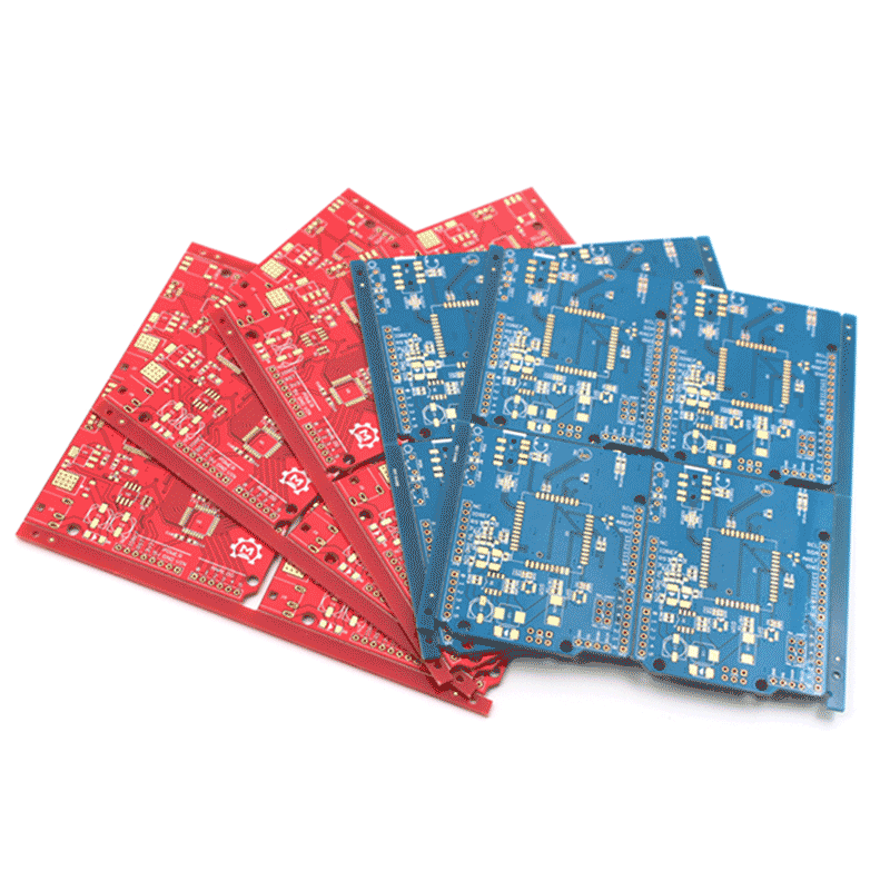
With more than 10 years experience in electronics manufacturing services(EMS), Makerfabs provide fast PCB prototyping service to makers, startups, engineers, and hobbyists, with the express PCB starting from $4.9 for 10 PCS! This is a good way for the makers& startups to get the PCBs for prototyping or trial-production, at a low price while the production and quality control follows all industrial standards.
How Does It work?
1. Go to our online-store PCB prototyping page, choose your options, include the PCB size, layers, color, finish, etc.
2. Verify that your Gerber files comply with all spec, and upload them.
3. Add to Cart. The system will calculate the final price for you.
For bigger quantities, more layers, special options, tests, panels, discounts or combination with our other services, contact us directly at service@makerfabs.com.
Gerber Files:
● pcbname.GTL: Top layer
● pcbname.GBL: Bottom layer
● pcbname.GTS: Solder Stop Mask top
● pcbname.GBS: Solder Stop Mask Bottom
● pcbname.GTO: Silk Top
● pcbname.GBO: Silk Bottom
● pcbname.TXT: NC Drill
● pcbname.GML: Mechanical layer
Spec:
● Layers: 1/2/4
● PCB Material: FR-4
● Thickness Tolerance: (t≥1.0mm) ± 10%
● Thickness Tolerance: (t<1.0mm) ± 0.1mm
● Insulation Layer Thickness: 0.075mm--5.00mm
● Minimum PCB track: 6mil
● Minimum Track/Vias Space: 6mil
● Minimum pads Space: 8mil
● Minimum silkscreen text size: 32mil
● Inner Layer Copper for 4-layer PCB: 17um
● Drilling Hole (Mechanical): 0.3mm—6.35mm
● Finish Hole (Mechanical): 0.8mm—6.35mm
● Drill Diameter Tolerance (unplated): 0.05mm
● Drill Diameter Tolerance (plated): 0.1mm
● Outline Tolerance (Mechanical): ±0.20mm
● Aspect Ratio: 8:1
● Solder Mask Type: Photosensitive ink
● SMT min Solder Mask Width: 0.2mm
● Min Solder Mask Clearance: 0.2mm
● Solder Mask Thickness: 15um
How Does It work?
1. Go to our online-store PCB prototyping page, choose your options, include the PCB size, layers, color, finish, etc.
2. Verify that your Gerber files comply with all spec, and upload them.
3. Add to Cart. The system will calculate the final price for you.
For bigger quantities, more layers, special options, tests, panels, discounts or combination with our other services, contact us directly at service@makerfabs.com.
Gerber Files:
● pcbname.GBL: Bottom layer
● pcbname.GTS: Solder Stop Mask top
● pcbname.GBS: Solder Stop Mask Bottom
● pcbname.GTO: Silk Top
● pcbname.GBO: Silk Bottom
● pcbname.TXT: NC Drill
● pcbname.GML: Mechanical layer
Note:
1. Note that Gerber files must be RS-274x format
2. Drill file(pcbname.TXT) should be Excellon format, and make sure it includes drills size and position data
3. Besides the production Gerber files, We also accept PCB files generated by Eagle, Altium Designer, PADS
4. Please leave a comment in the order for special requirements
Spec:
● PCB Material: FR-4
● Thickness Tolerance: (t≥1.0mm) ± 10%
● Thickness Tolerance: (t<1.0mm) ± 0.1mm
● Insulation Layer Thickness: 0.075mm--5.00mm
● Minimum PCB track: 6mil
● Minimum Track/Vias Space: 6mil
● Minimum pads Space: 8mil
● Minimum silkscreen text size: 32mil
● Inner Layer Copper for 4-layer PCB: 17um
● Drilling Hole (Mechanical): 0.3mm—6.35mm
● Finish Hole (Mechanical): 0.8mm—6.35mm
● Drill Diameter Tolerance (unplated): 0.05mm
● Drill Diameter Tolerance (plated): 0.1mm
● Outline Tolerance (Mechanical): ±0.20mm
● Aspect Ratio: 8:1
● Solder Mask Type: Photosensitive ink
● SMT min Solder Mask Width: 0.2mm
● Min Solder Mask Clearance: 0.2mm
● Solder Mask Thickness: 15um